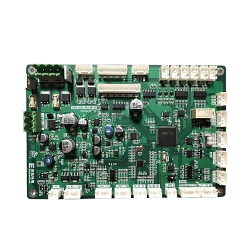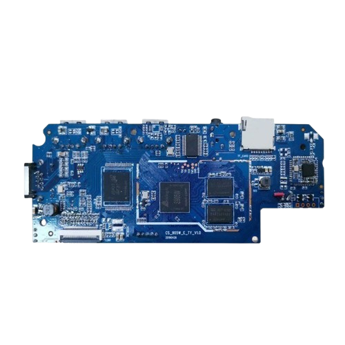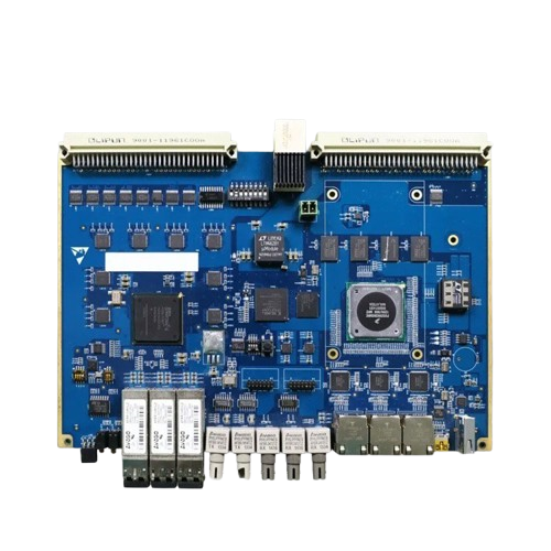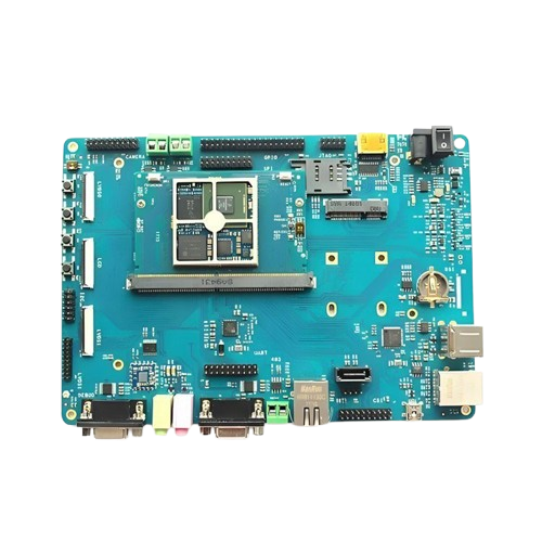
Aerospace PCB Assembly
In the aerospace industry, the choice of materials and components for circuit boards (PCBAs) is not a matter of chance. Imagine that these electronic devices have to go through the rocket launch of severe vibration, extreme temperature changes in space, and a strong radiation environment; ordinary materials simply can not withstand this “torture”.PCBA Basic Guidelines1.PCB substrateAerospace circuit board substrate must meet the four diamond standards:High-temperature resistance: to withstand extreme cold to the heat of repeated tortureCorrosion resistance: all kinds of radiation and chemicals in space can not hurt it a little bitGood insulation: signal transmission must be stable and reliableSturdy and durable: it can’t be broken even by the violent vibration during the launching.Commonly used “space-grade” materials include:Polyimide (PI): like a “bulletproof vest” for circuit boards, it is particularly resistant to high temperatures.Cyanoacrylate (CE): a well-balanced “top performer”.Ceramic substrate: first-class heat dissipation performance of the “cooling expert”.2.Component selection1. chip (IC) how to choose?Recognize the certification: QML-V/QML-Q certification is the “work permit”.Anti-radiation design: cosmic rays should have the “Golden Bell Mask”.Do not seek the latest but the most stable: 65nm or more mature process is more reliable2. Passive componentsCapacitors: Tantalum capacitors are the main force, ceramic capacitors should be COG/NPO type.Resistors: film resistors are the first choice, metal foil resistors have the best performance.Inductors: ferrite core or air core inductors are the most reliable.3. ConnectorsStandard: MIL-DTL-38999/32139 is the basic requirement.Gold plating: Contacts must be plated with at least 50 micro inches of gold.Double insurance: must be with secondary locking mechanism3.Special ProcessesEncapsulation technologyCeramic package is the first choice, like a “spacesuit” for the chip.Plastic packages must be certified by the militaryBGA packages should not be used unless specially reinforcedSolderingTraditional high Pb solder (Sn63Pb37) still dominantIf lead-free process is used, additional verification is requiredX-ray “checkup” after soldering to make sure there are no “internal injuries”.Protective treatmentsCoatings must comply with military standard MIL-I-46058.Parylene coatings are most effectiveThe thickness of the coating should be controlled within the range of the thickness of a hair.4.Supply Chain ManagementPurchasing ChannelOnly take goods from the original factory or authorized distributorsResist counterfeit componentsEach component should have an “ID card”, the whole process can be traced.Quality Inspection100% inspection of incoming materials, no one can be left outRandom disassembly testing, no less than 10%.Accelerated aging test to predict the service lifeChange managementAny change must be re-verifiedChanging components equals to re-certificationAll change records should be kept completelyAerospace PCBA soldering process 1.Soldering ProcessIn the aerospace field, an unqualified solder joint can be the “Achilles heel” of the entire mission. As the equipment has to experience repeated “torture” from extreme cold to extreme heat, the welding process must be foolproof.1. Welding process: three big diamondsWave soldering: suitable for high-volume through-hole component welding, like a roller coaster, with the PCB passing through the molten solderReflow soldering (mainstream choice): accurate “local heating” technology, especially suitable for chip componentsSelective wave soldering: “Precision spot soldering” technology for specific solder joints.2. Reflow processTemperature profiles are key: like baking a cake, too high a temperature will burn, too low a temperature will undercook itParameter customization: different materials and components require different “cooking solutions”.Solder paste selection: to choose the special formula for aerospace-grade, ordinary solder paste simply can not carry the space environment2.Aviation-grade circuit board processing1. Precision control: the ultimate pursuit of micron-levelLaser positioning: accuracy of ± 5 microns (equivalent to 1/10 of a hair)Optical alignment: Angular error less than 0.001 degrees (more accurate than a compass)Surface treatment: copper foil smoothness comparable to mirror (Ra≤0.3μm)2. Reliability Verification: Tougher tests than the space environmentTemperature torture test: -65℃ to 150℃ repeatedly tossed 1000 timesVibration test: simulate the violent vibration of a rocket launchVacuum test: 10-⁶ torr vacuum under the extreme testAging test: 85 ℃ / 85% humidity under the continuous “sauna” for 1000 hours3.Quality ControlProcess monitoring: real-time monitoring of each key parameter like a medical checkup.Traceability system: each board has an “ID card”, and the whole process can be traced.Certification standards: meet the most stringent aviation quality standards (AS9100D, etc.)4.S pecial ProcessMicroporous Processing: Laser-punched holes thinner than a hairline (±10μm precision).High-frequency signal processing: impedance control accurate to ±3% (comparable to laboratory instruments)Three-stage inspection: self-inspection + inspection + final inspection, to ensure that nothing is lost.## Aerospace PCBA Surface FinishesIn the space environment, circuit boards face challenges far beyond those of terrestrial applications. To ensure reliable long-term operation, special “protection suits” must be used:1. Metal protective layer (anti-corrosion treatment)Electroless nickel/impregnated gold (ENIG): like a “golden armor” for circuits, it protects against rust and ensures good conductivity.Electroless nickel/gold plating (ENEPIG): more advanced “composite armor”, especially suitable for high reliability requirements.Characteristics: anti-oxidation, corrosion resistance, to ensure that the connector contact remains as new.2.Organic protective layer (all-round protection)Polyimide (PI) coating: aerospace-grade “protective clothing”, high temperature resistance up to 300 ℃ or moreSilicone potting: sensitive circuits to wear “anti-vibration airbag”, buffer mechanical shockEffect: moisture-proof, shock-proof, radiation-proof, triple protection in one step.Rigorous product testing1. Environmental Adaptability TestTemperature endurance race:High and low temperature cycle (-65℃~150℃ repeated tossing)Temperature shock (instantaneous switching of extreme temperatures)Mechanical strength test:Vibration test (simulate the violent vibration of a rocket launch)Shock test (1500G acceleration shock)2. Electrical performance verificationFlying needle test: like a “master acupuncturist” to accurately detect each nodeTest Rack Verification: Comprehensive “physical examination” to ensure that all functions are normal.Signal integrity: high-frequency signal transmission quality analysis3. Accelerated aging testLife Prediction: Accelerated aging through a high temperature and high humidity environment.Continuous monitoring: record the trend of performance parametersFailure analysis: Use an electron microscope to find out potential defects.In conclusion, the special process requirements of aerospace PCBA are reflected in material selection, welding process, surface treatment, protective measures and test verification, and other aspects. Only by strictly following these requirements and constantly carrying out technological innovation and process improvement can we manufacture PCBA products to meet the needs of the aerospace field.