12-Layer PCB
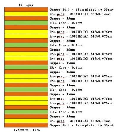
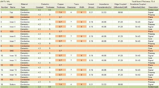
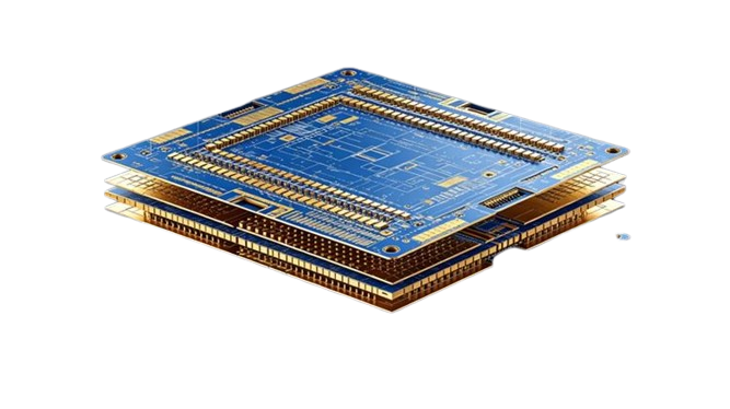
In most projects, engineers do not move to a 12 layer PCB simply because they want more routing layers. The real reason is usually signal integrity, power stability, BGA breakout complexity, or EMI control has already reached the limit of an 8 or 10 layer stackup.This is especially common in FPGA platforms, industrial computing systems, AI modules, telecom hardware, and high-speed embedded devices. Once DDR routing, differential pairs, power planes, shielding, and thermal constraints start competing for space, lower-layer boards become increasingly difficult to manage.We often see this during DFM reviews. The schematic may be correct, but the stackup structure itself creates manufacturing or electrical risks later in production.A well-designed 12-layer PCB is not just about adding layers. It is about creating a stable electrical structure that can support high-speed signals, maintain clean return paths, reduce EMI, and remain mechanically reliable after multiple thermal cycles.For companies developing advanced multilayer boards, our main Multilayer PCB Manufacturing page also covers additional stackup and fabrication capabilities.Why Engineers Move to a 12 Layer PCBIn real production environments, the transition from 10 layers to 12 layers usually happens for three reasons:High pin-count BGA routing becomes congestedPower and ground reference layers are no longer sufficientSignal integrity problems appear during testingMany modern processors and FPGAs require dedicated reference planes for stable impedance control. If you force all the routing into fewer layers, you often get split return paths, too many vias, crosstalk and unstable impedance behaviour.Following a thorough review of multiple networking and industrial controller projects, it became evident that the primary concern was not the routing density itself, but rather the substandard continuity of the reference plane under high-speed differential pairs.Once data rates increase, the stackup becomes part of the electrical design — not just the manufacturing structure.Typical 12 Layer PCB Stackup StrategyThere is no universal 12 layer stackup. The correct structure depends heavily on:Signal speedBGA densityBoard thicknessImpedance targetsPower distribution requirementsEMI performance goalsBut in practice, symmetrical stackups are still the go-to because they reduce warpage during lamination and reflow.A common approach is:LayerFunctionL1SignalL2GroundL3High-Speed SignalL4SignalL5PowerL6GroundL7GroundL8PowerL9SignalL10High-Speed SignalL11GroundL12SignalThis structure enables high-speed layers to remain in proximity to solid reference planes, thereby maintaining relatively stable power distribution.In thicker 12 layer boards, engineers also need to pay attention to resin balance and copper distribution. Uneven copper density across layers is one of the common causes of board twist and warpage after assembly.Impedance Control Is Usually the Real ChallengeMany customers assume impedance control is mainly about trace width calculation. In practice, the stackup consistency is often the more difficult part.For instance, altering the prepreg combinations from 1080 to 2116 could affect the impedance sufficiently to necessitate adjustments to the line width.On high-speed 12 layer designs, several factors interact simultaneously:Copper roughnessGlass weave effectDielectric thickness toleranceEtching compensationResin flow during laminationReference plane continuityWe generally advise that high-speed differential pairs should be maintained between solid ground references, as opposed to routing adjacent to split power planes. This is particularly relevant in thick multilayer boards, where the control of return path discontinuity can become more challenging.For PCIe, DDR, or SerDes applications, backdrilling may also be necessary to reduce via stub effects.This becomes more important once signal speeds move beyond traditional industrial control frequencies.Via Design Starts Affecting Yield Much Earlier Than ExpectedOne thing many engineers underestimate on 12 layer boards is via structure complexity.For many industrial products, a standard through-hole structure remains the most reliable and cost-effective option. However, once large BGAs are introduced, blind vias and buried vias quickly become necessary.This creates additional manufacturing considerations:Sequential laminationLaser drilling accuracyRegistration toleranceCopper filling reliabilityCAF resistanceAspect ratio limitationsFor example, a thick 12 layer board with small mechanical drill sizes may easily exceed recommended aspect ratios. If you go too far with the drilling, the hole walls and the plating can’t stand the test of time.In some telecoms and server projects, we have seen reliability issues caused not by the layout itself, but by via dimensions that were over-optimised and pushed the limits of manufacturing too far.If HDI structures are required, our HDI PCB Manufacturing capability page explains additional process options.Material Selection Matters More on 12 Layer BoardsOn lower-layer boards, standard FR4 is usually sufficient.The behaviour of the material becomes much more noticeable on 12-layer PCBs because the board experiences multiple lamination cycles and higher thermal stress during assembly.High Tg materials are often preferred for industrial and automotive applications because they improve dimensional stability during thermal cycling.Once insertion loss starts affecting signal performance, low-loss materials become important for high-speed systems.Common material combinations may include:FR4 Tg170Panasonic Megtron seriesIsola low-loss laminatesRogers hybrid stackupsMaterial selection also directly affects:Impedance stabilityZ-axis expansionCAF resistanceDelamination riskDrilling qualityIn actual production, selecting the incorrect prepreg combination can cause more issues than selecting the incorrect copper weight.Lamination Stability Is One of the Biggest Manufacturing RisksA 12 layer PCB is not manufactured the same way as a simple multilayer board.The more layers involved, the more sensitive the process becomes to:Resin flowPress cycle parametersLayer alignmentMaterial expansionInner-layer oxide treatmentCopper balancingThis is why experienced multilayer PCB manufacturers devote considerable time to reviewing stackup symmetry before production begins.Poor lamination control may lead to:DelaminationVoid formationExcessive warpageBarrel crackingResin starvationEven minor lamination defects in high-reliability sectors such as telecommunications and aerospace electronics can eventually lead to field failures under long-term thermal cycling.DFM Review Becomes Critical on 12 Layer PCB ProjectsOne of the most common issues we encounter is electrically functional designs, yet difficult to manufacture consistently.A few examples include:Extremely uneven copper distributionExcessive via density under BGA areasOverly thin annular ringsTight drill-to-copper clearanceImpedance traces crossing split planesStacked vias without sufficient fill process capabilityFor complex multilayer projects, a DFM review should be carried out before the final Gerber release, rather than after fabrication issues arise. Even minor changes to the stackup or routing strategy can greatly enhance manufacturing yield and long-term reliability.Our PCB Design Service team often works with customers during this stage to optimise manufacturability before production begins.Where 12 Layer PCBs Are Commonly UsedToday, 12 layer PCBs are widely used in systems where electrical stability and routing density are both critical.Typical applications include:FPGA development platformsIndustrial automation controllersAI computing hardwareTelecom infrastructureMedical imaging systemsAutomotive radar electronicsEmbedded computing platformsHigh-speed networking equipmentCompared with lower-layer boards, a 12-layer structure that has been designed properly offers better EMI suppression, cleaner reference planes and more predictable signal behaviour.FAQQ: What thickness is typical for a 12 layer PCB?A: Most 12 layer PCBs fall between 1.6mm and 3.2mm, depending on copper weight, impedance requirements, and via structure design.Q: Are 12 layer PCBs always HDI boards?A: No. Many 12 layer boards still use standard through-hole structures. HDI becomes necessary mainly when BGA density or routing constraints increase significantly.Q: What is the biggest issue in 12 layer PCB manufacturing?A: In practical production, achieving lamination stability and impedance consistency is usually more challenging than routing.Q: Is standard FR4 suitable for 12 layer PCB projects?A: For many industrial applications, yes. However, high-speed or thermally demanding systems may require high Tg or low-loss materials.Q: Why does 12 layer PCB cost increase significantly?A: The main reasons for the cost increase are additional lamination cycles, tighter registration tolerances, greater drilling complexity, impedance testing and lower manufacturing yield margins.