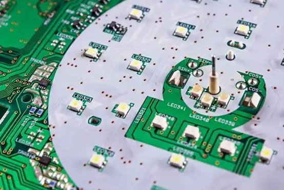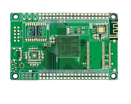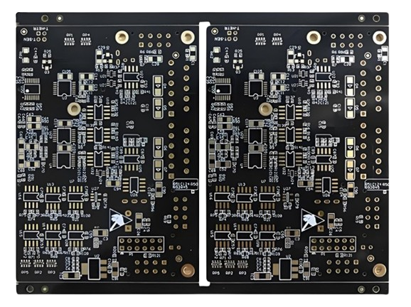


High-speed circuit boards are circuit boards used for high-speed signal transmission. They are specially designed to process high-frequency and high-rate electrical signals to ensure the accuracy and stability of data during high-speed transmission. Their main characteristics include high frequency performance, low loss, and excellent heat dissipation.
Definition & Key Features
Application | Frequency | Typical Material | Special Process |
5G AAU Modules | 24-47GHz | Rogers RO4835 | Laser Drilling + HDI Stackup |
Data Center Switches | 56Gbps PAM4 | Megtron6 | Ultra-Low Profile Copper |
Automotive Radar | 77-81GHz | Taconic RF-35 | Embedded Capacitors/Resistors |
High-speed PCB board parameters
Item | Rigid PCB |
Max Layer | 60L |
Inner Layer Min Trace/Space | 3/3mil |
Out Layer Min Trace/Space | 3/3mil |
Inner Layer Max Copper | 6oz |
Out Layer Max Copper | 6oz |
Min Mechanical Drilling | 0.15mm |
Min Laser Drilling | 0.1mm |
Aspect Ratio(Mechanical Drilling) | 20:1 |
Aspect Ratio(Laser Drilling) | 1:1 |
Press Fit Hole Ttolerance | ±0.05mm |
PTH Tolerance | ±0.075mm |
NPTH Tolerance | ±0.05mm |
Countersink Tolerance | ±0.15mm |
Board Thickness | 0.4-8mm |
Board Thickness Tolerance(<1.0mm) | ±0.1mm |
Board Thickness Tolerance(≥1.0mm) | ±10% |
Impedance Tolerance | Single-Ended:±5Ω(≤50Ω),±7%(>50Ω) |
Differential:±5Ω(≤50Ω),±7%(>50Ω) | |
Min Board Size | 10*10mm |
Max Board Size | 22.5*30inch |
Contour Tolerance | ±0.1mm |
Min BGA | 7mil |
Min SMT | 7*10mil |
Surface Treatment | ENIG,Gold Finger,Immersion Silver,Immersion Tin,HASL(LF),OSP,ENEPIG,Flash Gold;Hard gold plating |
Solder Mask | Green,Black,Blue,Red,Matt Green |
Min Solder Mask Clearance | 1.5mil |
Min Solder Mask Dam | 3mil |
Legend | White,Black,Red,Yellow |
Min Legend Width/Height | 4/23mil |
Strain Fillet Width | / |
Bow & Twist | 0.3% |
Golden Rules for Design Optimization
Parameter | Recommended Value | Engineering Basis |
Ground Via Spacing | λ/10@Max Frequency | Prevents resonance |
Anti-Pad Size | Via Diameter + 20mil | Reduces capacitive discontinuity |
Back-Drilling Depth | Target Layer + 2mil | Eliminates stub effects |
Cutting-Edge Technologies
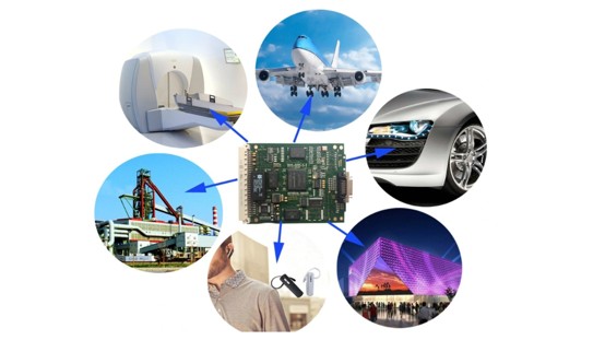
Application of PCB
PCB application in consumer electronics, Aerospace, Telecom communication, military and defense, Industrial control, automotive industry.
Our Full-Capability Offerings
Advanced PCB Technologies
Precision PCBA Services
Engineering Design Support
Specialized Manufacturing Capabilities
Technology | Key Specifications | Typical Applications |
HDI Microvia | 50μm laser drills | 5G mmWave devices |
Embedded Passives | 0201 discrete components | Aerospace avionics |
RF Microwave | ±0.1mm impedance control | Radar systems |
Why Partner With Us?
✔ One-Stop Solution – From design to box-build assembly
✔ NPI Acceleration – 15-day standard lead time for prototypes
✔ Global Certifications – IATF 16949, ISO 13485, UL certified
Value-Added Services
• Free Design Review – Our engineers analyze your files within 4 business hours
• Cross-Platform Support – Accepts Altium, Cadence, PADS, and Mentor designs
• Supply Chain Integration – Component sourcing with 98% first-pass success rate