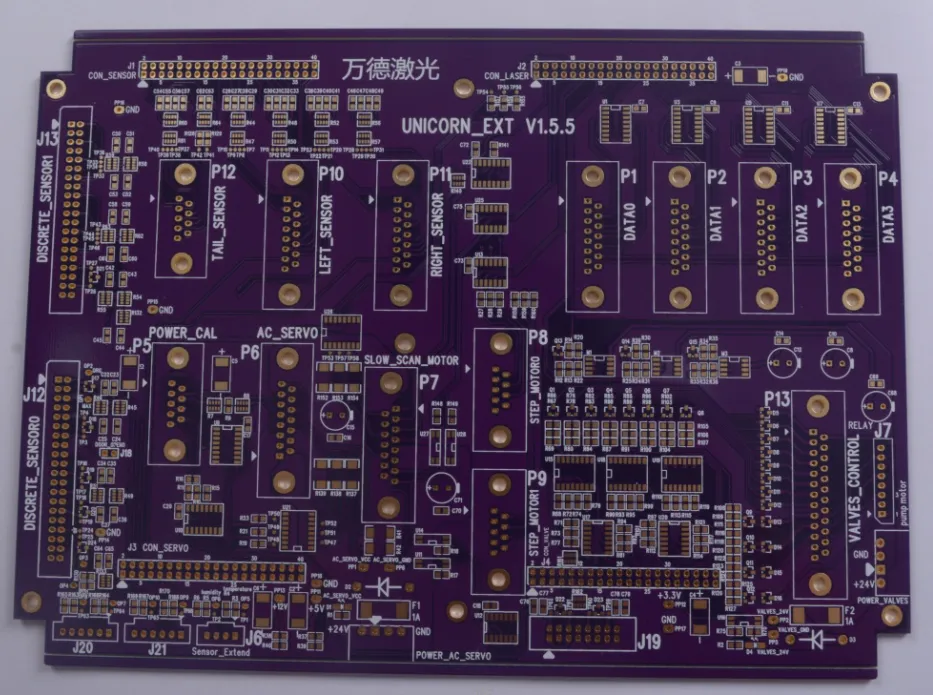


In today’s electronic product design, 4-layer 1.6 mm PCBs have become the preferred solution for many engineers. This structure strikes a perfect balance between complexity, cost, and performance, making it particularly suitable for medium-complexity circuit designs.
Standard Stackup Structure of 4-Layer 1.6mm PCB
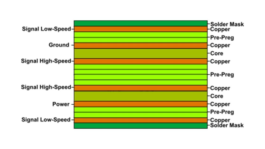
The standard 4-layer 1.6mm PCB typically adopts the classic “signal layer/ground layer/power layer/signal layer” configuration with the following arrangement:
Bottom Layer (L4): Signal layer (outer), for auxiliary routing and component placement
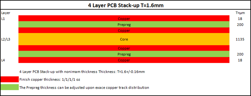
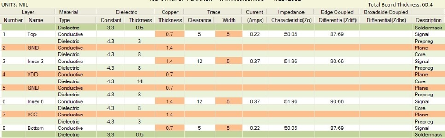
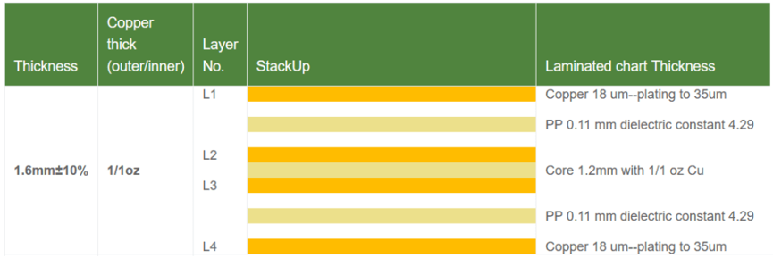
This structure uses prepreg (PP, typically 2116 type, about 0.12mm thick) to laminate the layers together, forming a finished board with a total thickness of 1.6mm. A typical material thickness distribution example is as follows:
Layer | Material/Description | Thickness (Example) |
Top Layer | Signal layer (1oz copper) | 0.035mm |
Prepreg | Dielectric (FR-4) | 0.2mm |
Inner Layer 1 | Ground plane (1oz copper) | 0.035mm |
Core | Dielectric (FR-4) | 0.8mm |
Inner Layer 2 | Power plane (1oz copper) | 0.035mm |
Prepreg | Dielectric (FR-4) | 0.2mm |
Bottom Layer | Signal layer (1oz copper) | 0.035mm |
Historical Origins of 1.6mm Thickness as Industry Standard
The 1.6mm (approximately 63mil) thickness becoming an industry standard for PCBs is no coincidence but has deep historical roots. During the vacuum tube era, phenolic resin laminates were typically produced at 1/16 inch (about 1.6mm) thickness, and matching connectors and other components were designed for this specification, gradually forming a complete industrial chain standard.
With technological advancements, although PCB thickness ranges have now expanded to 0.4-3.0mm or even wider, 1.6mm remains the default choice for most electronic products due to its good mechanical strength, manufacturing convenience, and cost-effectiveness. Especially for 4-layer boards, 1.6mm thickness provides ideal interlayer insulation and structural stability.
Key Design Considerations for 4-Layer 1.6mm PCB
Impedance Control and Signal Integrity
In high-speed circuit design, impedance control is crucial. The 4-layer 1.6mm PCB provides clear reference planes for signals through dedicated ground and power layers, greatly simplifying impedance matching design. Typical design values include:
By precisely controlling trace width (e.g., 0.195mm), spacing, and dielectric thickness, engineers can easily achieve target impedance values. TUOGEE’s engineering team has extensive experience in impedance control and can provide professional advice for your design.
Power Distribution and Decoupling Design
The advantages of dedicated power layers include:
It is recommended to place decoupling capacitors of appropriate values near power pins to form a low-impedance power distribution network (PDN).
Electromagnetic Compatibility (EMC) Optimization
The stackup structure of 4-layer 1.6mm PCBs naturally provides good EMC performance:
Material Selection and Performance Parameters
Core Material Options
Key Performance Parameters
Comparison and Applications of 4-Layer PCBs with Different Thicknesses
While 1.6mm is the industry standard, other thicknesses have their applicable scenarios:
Thickness | Characteristics | Typical Applications |
0.8mm | Space-saving, more flexible | Portable devices, small consumer electronics |
1.0mm | Balanced thickness and strength | Industrial control modules, communication equipment |
1.2mm | Moderate mechanical strength | Automotive electronics, medical devices |
1.6mm | Standard thickness, best cost-performance ratio | Most consumer and industrial electronics |
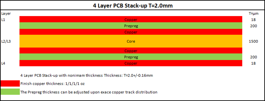
2.0mm+ | Ultra-high mechanical strength | Power modules, heavy-duty equipment |
It’s worth noting that non-standard thicknesses (such as 0.8mm or 2.0mm) may require additional costs and should be considered comprehensively at the design stage.
Manufacturing Process and Quality Control Points
The manufacturing process for 4-layer 1.6mm PCBs includes:
TUOGEE employs advanced AOI (Automated Optical Inspection) and flying probe testing to ensure the quality of each PCB, with impedance control accuracy reaching ±7%, far exceeding the industry standard of ±10%.
Frequently Asked Questions
Q: Why do most interface standards adapt to 1.6mm thickness?
A: This is an industry standard formed historically, as early connectors were designed for 1/16 inch (≈1.6mm), and the supporting industrial chain developed accordingly.
Q: How much more expensive is a 4-layer 1.6mm PCB compared to a double-sided board?
A: Typically 1.5-2 times the cost of double-sided boards, but through design optimization (such as standard stackup) and volume production, TUOGEE can offer highly competitive prices.
Q: How to determine whether my project needs 1.6mm or other thicknesses?
A: Consider factors including: mechanical strength requirements, connector compatibility, thermal requirements, and cost budget. TUOGEE engineers can provide free evaluations.
Recommendations for Selecting Professional PCB Manufacturing Services
When choosing a PCB manufacturer, pay attention to:
As a professional PCB manufacturer, TUOGEE has 17 years of experience in producing 4-layer boards, offering comprehensive services from design support to mass production. We specialize in the precision manufacturing of 1.6mm thick PCBs, offering industry-leading impedance control accuracy.
Get Your Custom PCB Solution Now:
Contact TUOGEE Engineers | Online Quotation System
Whether you need standard 1.6mm 4-layer boards or custom thicknesses, TUOGEE can provide high-quality, highly reliable products to help successfully implement your electronic projects.