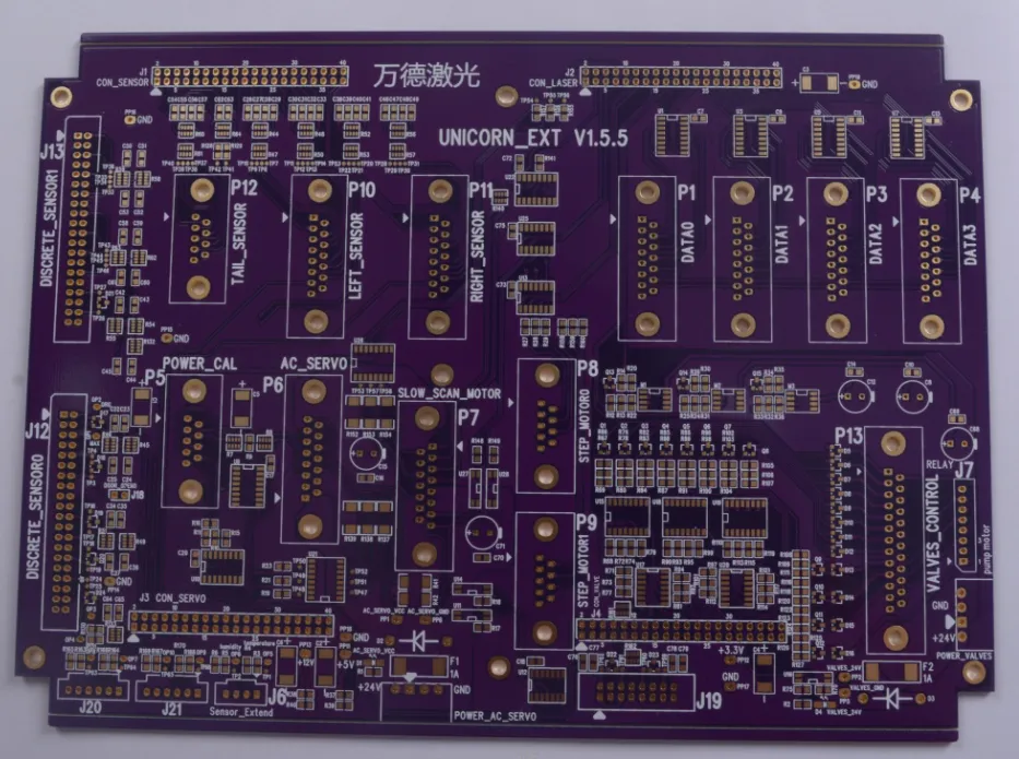


Once a project reaches 14 layers, the PCB is no longer just a circuit carrier. At this stage, the board itself becomes part of the signal integrity, thermal, and power distribution strategy.
Most engineers move to a 14 layer PCB because lower-layer stackups can no longer support routing density, reference plane continuity, or EMI requirements without compromising reliability.
This is common in:
Compared with 10 or 12 layer boards, a 14 layer PCB introduces much tighter manufacturing tolerances. Small problems that are manageable on lower-layer designs often become yield or reliability risks once the stackup becomes thicker and more complex.
For additional multilayer fabrication capabilities, you can also explore our Multilayer PCB Manufacturing page.
Why 14 Layer PCBs Are Increasingly Common
Modern electronic systems are pushing routing density much harder than before.
On several recent FPGA and AI projects we reviewed, the issue was not component placement itself, but maintaining stable reference planes while handling dense BGA escape routing and multiple high-speed interfaces simultaneously.
A 14 layer stackup gives engineers more flexibility to separate:
This separation improves both signal stability and EMI performance.
In practice, many 14 layer boards are designed not because engineers need “more layers,” but because they need cleaner electrical behavior under higher data rates.
Stackup Planning Becomes a Critical Engineering Decision
At the 14 layer level, stackup planning should happen before layout work begins.
Poor stackup decisions often create problems later such as:
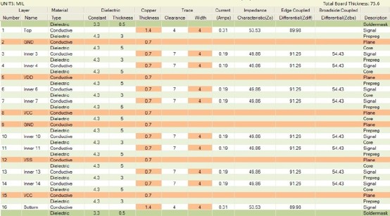
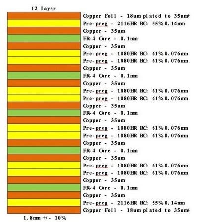
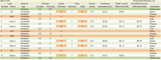
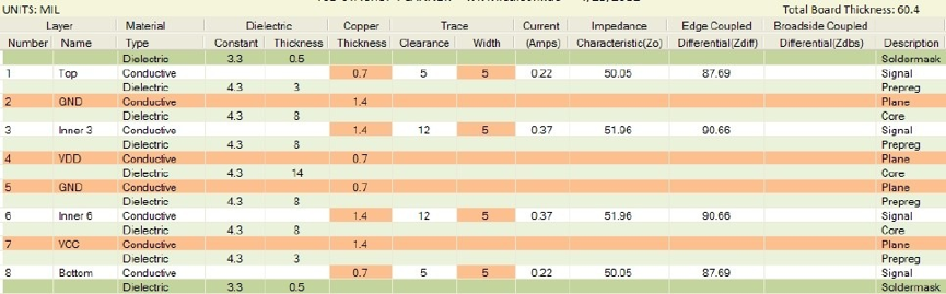
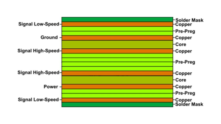
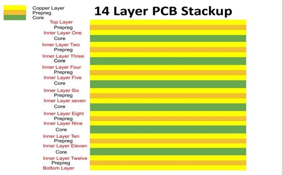
A typical 14 layer PCB stackup may look like this:
Layer | Function |
L1 | Signal |
L2 | Ground |
L3 | High-Speed Signal |
L4 | Signal |
L5 | Power |
L6 | Ground |
L7 | Signal |
L8 | Signal |
L9 | Ground |
L10 | Power |
L11 | Signal |
L12 | High-Speed Signal |
L13 | Ground |
L14 | Signal |
The exact structure depends heavily on:
In actual manufacturing, symmetrical copper distribution is extremely important. Uneven copper balance across 14 layers can easily create twist and bow issues during assembly reflow.
Signal Integrity Problems Become More Difficult to Hide
On lower-layer boards, some routing mistakes may still pass testing without obvious issues.
On 14 layer PCBs running high-speed interfaces, the margin becomes much smaller.
We frequently see problems related to:
For PCIe Gen4, DDR4/DDR5, or high-speed SerDes channels, the stackup and routing structure directly affect overall system stability.
Backdrilling is also becoming more common on 14 layer boards because via stubs start creating measurable signal degradation at higher frequencies.
In practical production, impedance control is usually less about calculation formulas and more about maintaining manufacturing consistency across the entire stackup.
HDI Structures Are Often Necessary on 14 Layer Boards
Large BGAs and dense routing areas often make standard through-hole routing impractical.
As a result, many 14 layer PCB projects introduce:
These technologies improve routing density but significantly increase fabrication complexity.
One common issue is over-aggressiveness via sizing. Engineers sometimes reduce drill sizes too aggressively without considering manufacturing capability or plating reliability.
For thicker multilayer boards, drill aspect ratio becomes a serious reliability factor.
A structure that looks electrically optimized may still create:
For advanced technologies, our HDI PCB Manufacturing service page explains additional fabrication capabilities.
Material Selection Directly Affects Reliability
At 14 layers, material behavior becomes much more important than many engineers initially expect.
Multiple lamination cycles, thicker stackups, and higher assembly temperatures all increase stress on the PCB structure.
For industrial and telecom systems, high Tg materials are commonly used to improve dimensional stability during thermal cycling.
For high-speed designs, low-loss materials help reduce insertion loss and signal degradation.
Common material options include:
Material choice affects:
In real production environments, incorrect prepreg combinations often create more reliability problems than routing itself.
Thermal Management Cannot Be Ignored
Many 14 layer boards support processors, FPGAs, AI chips, or power-intensive devices.
As layer count increases, heat dissipation becomes more difficult because thicker PCB structures trap thermal energy more easily.
Thermal management strategies may include:
Without proper thermal planning, localized hotspots may create long-term reliability issues even if the board passes initial testing.
Lamination Stability Is One of the Hardest Manufacturing Challenges
A 14 layer PCB requires significantly tighter process control than standard multilayer boards.
The lamination process must control:
Even slight process variation may lead to:
This becomes especially critical on large-format telecom or server boards where mechanical stress increases across the panel.
Several multilayer failures we investigated were ultimately related to lamination imbalance rather than electrical design errors.
How to Improve 14 Layer PCB Reliability
Many signal integrity problems originate from interrupted return current paths rather than trace routing itself.
High-speed layers should remain adjacent to continuous ground references whenever possible.
Every via transition introduces discontinuity.
Keeping critical signals on fewer layers often improves performance more than aggressive impedance tuning.
Small drill sizes on thick boards may exceed reliable plating capability.
This is especially important for telecom and industrial products with long service life requirements.
Copper imbalance is a major source of multilayer PCB warpage.
Balancing copper density early in layout usually improves manufacturing stability significantly.
At the 14-layer level, DFM review should happen during layout — not after fabrication problems appear.
Critical review points include:
. Drill-to-copper clearance
. Annular ring tolerance
. Resin flow risk
. Impedance manufacturability
. Via reliability
. Copper balancing
. Registration capability
Our PCB Design Service team often supports customers during this optimization stage.
Typical Applications for 14 Layer PCBs
14 layer PCB boards are commonly found in:
As data rates continue increasing, more embedded systems are moving toward higher-layer-count PCB architectures to maintain electrical stability.
FAQ
Q: What is the standard thickness of a 14 layer PCB?
A: Most 14 layer PCBs range from approximately 2.0mm to 3.2mm, depending on stackup design, copper weight, and impedance requirements.
Q: Are 14 layer PCBs always HDI designs?
A: Not always. However, many dense BGA applications require blind vias or buried vias to maintain routing efficiency.
Q: What causes warpage on 14 layer PCBs?
A: Uneven copper distribution, poor lamination balance, and improper material selection are among the most common causes.
Q: Why are low-loss materials often used on 14 layer boards?
A: Higher data rates create greater insertion loss, making low-loss materials important for maintaining signal quality.
Q: What is the biggest manufacturing challenge for 14 layer PCBs?
A: In practical production, lamination stability and registration accuracy are usually among the most difficult process controls.
Conclusion
A 14 layer PCB is typically used when electrical performance, routing density, and long-term reliability all become equally important.
At this level, successful PCB manufacturing depends not only on layout quality but also on stackup planning, material selection, via strategy, and realistic manufacturability considerations.
The most reliable multilayer designs are usually the ones developed with both electrical performance and fabrication capability in mind from the beginning.