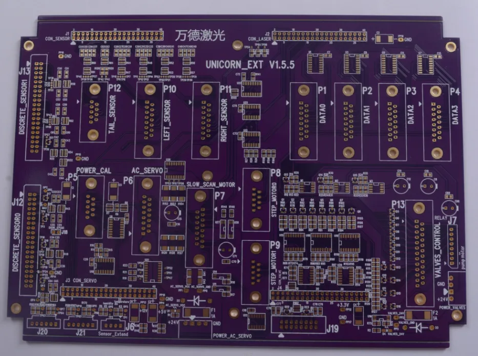


As the “backbone” of electronic products, PCB technology must evolve in tandem to meet increasingly demanding requirements. With its superior multi-layer architecture and signal integrity advantages, the 8-layer PCB has become an indispensable key component in modern high-end electronic devices.
Architectural advantages of 8-layer PCBs
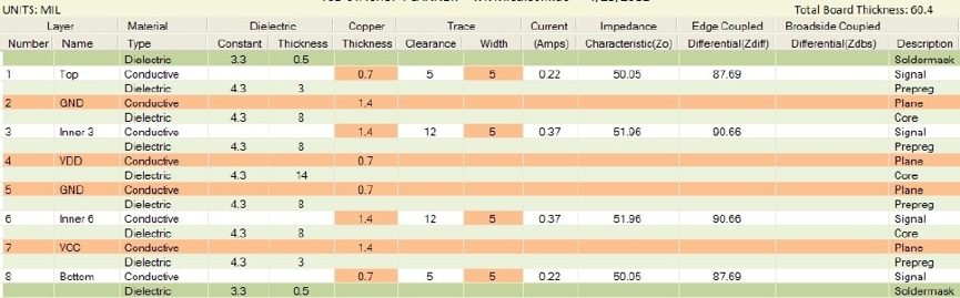
1. Precision Stack-Up Design
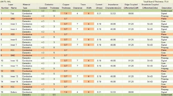
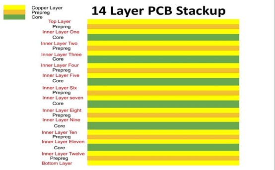
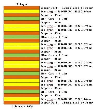
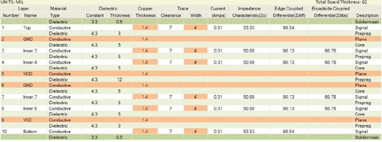
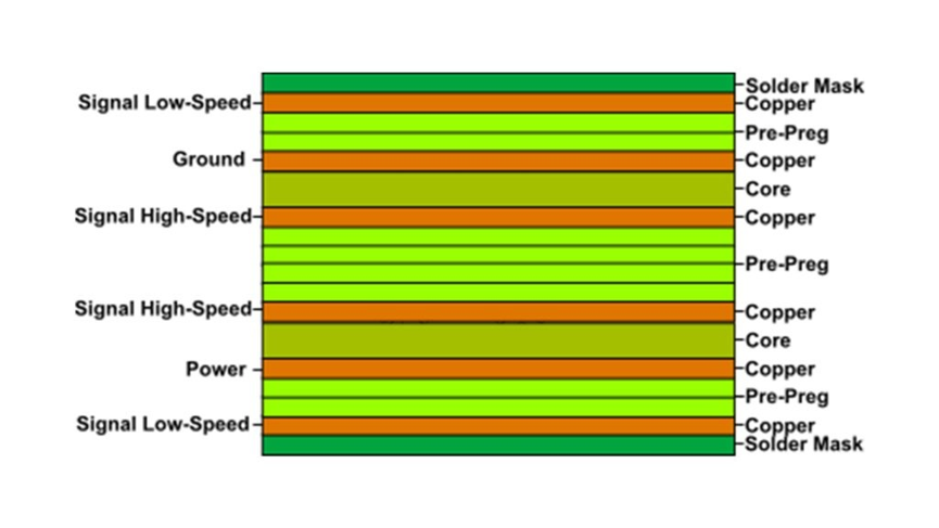
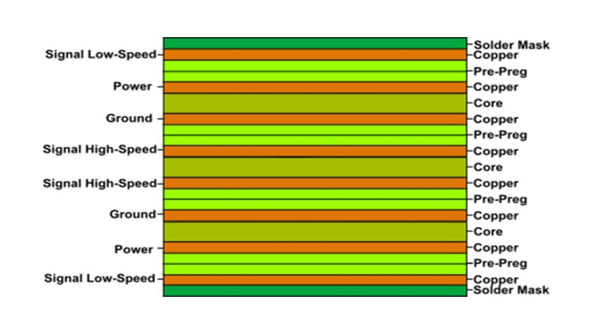
Our 8-layer PCBs adopt an industry-leading “2-4-2” symmetrical stack-up structure:
This structure ensures:
✓ Excellent EMI shielding performance (15-20dB reduction in radiation)
✓ Impedance control accuracy within ±5%
✓ 30%+ improvement in crosstalk suppression
2. Signal Integrity Optimization
Key parameters for high-speed design:
Compatible with DDR4/DDR5 memory interfaces
Breakthrough Applications in Material Science
1. High-Performance Substrate Options
We offer multiple material solutions for different needs:
2. Copper Foil Technology Innovation
Using Reverse Treat Foil (RTF) technology:
The Pursuit of Manufacturing Excellence
1. High-Precision Processing Capabilities
2. Advanced Surface Finishes
Optimal solutions for different applications:
Typical Applications and Solutions
1. 5G Communication Equipment
2. AI Hardware
3. Automotive Electronics
In-vehicle networks: High-speed bus design
Reliability Verification System
We have established a comprehensive quality assurance system:
Customer Support Ecosystem
We provide full-range technical support:
“By choosing our 8-layer PCB solutions, you gain:
✓ Support from signal integrity experts
✓ Proven reliable design solutions
✓ Flexible production capacity
✓ Competitive lead times and costs”
Contact our technical consultants today for customized 8-layer PCB solutions tailored to your project!