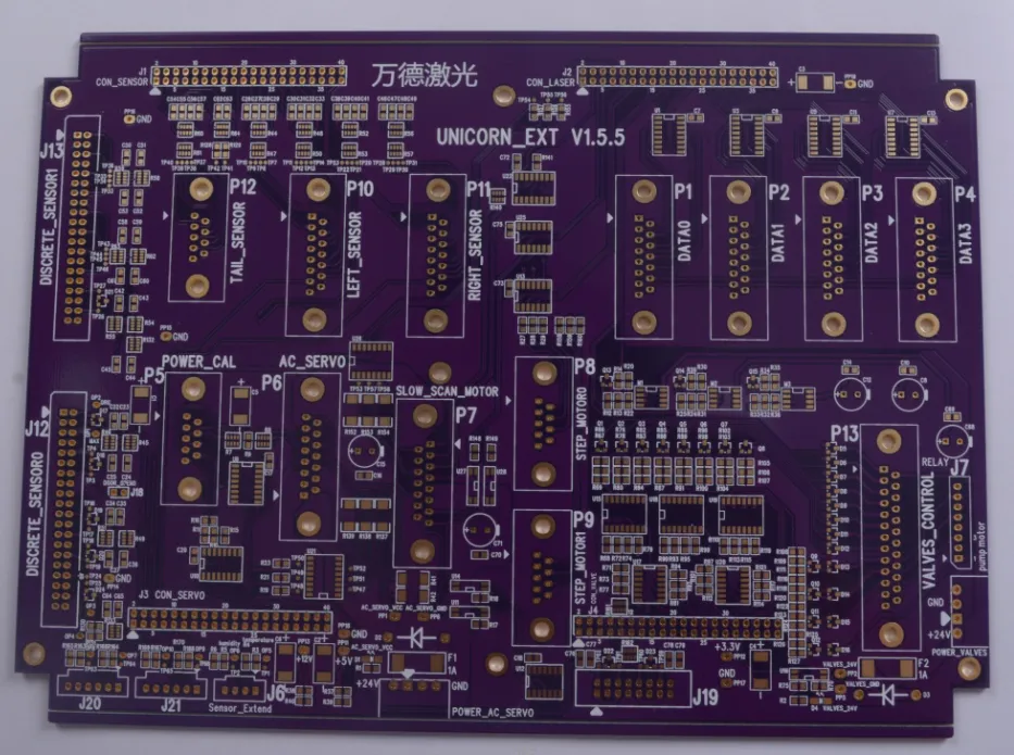


Introduction to 6-Layer PCBs
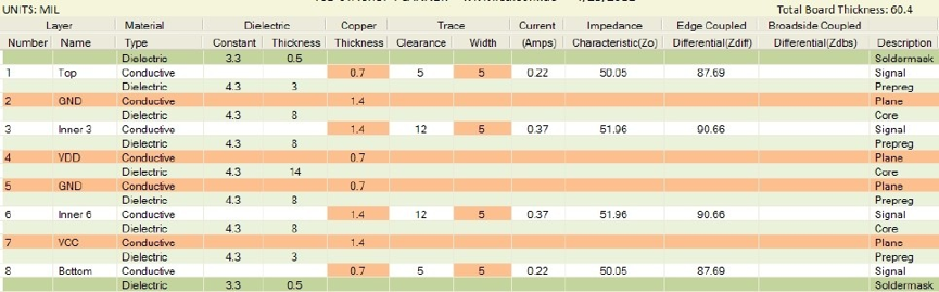
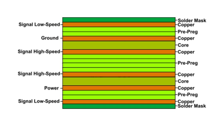
A six-layer PCB is a multi-layer printed circuit board made of six alternating layers of conductive copper foil and insulating material. This innovative design is amazing! It enables the creation of complex circuits through precise internal layer connection technology, making it ideal for high-performance electronic devices. They include signal layers, power layers, and ground layers. These layers are laid out in the best way so that signal integrity and electromagnetic compatibility are optimized.
6-layer boards are simply amazing! They offer more routing space and better noise suppression capabilities than four-layer boards. This makes them perfect for high-speed digital circuits, RF communications, and other applications.
TUOGEE employs advanced microvia technology and precision lamination processes to ensure the high reliability and stability of six-layer boards.
Advantages of 6-Layer PCBs
Advantage | Description |
High-Density Routing | Microvia technology enables finer trace layouts, saving space |
Excellent Signal Integrity | Dedicated power/ground planes reduce crosstalk and enhance high-frequency performance |
Superior Thermal Management | Thermal vias and copper layers distribute heat evenly |
Enhanced Mechanical Stability | A multilayer structure improves resistance to bending and vibration |
Design Flexibility | Supports blind/buried vias for complex circuit requirements |
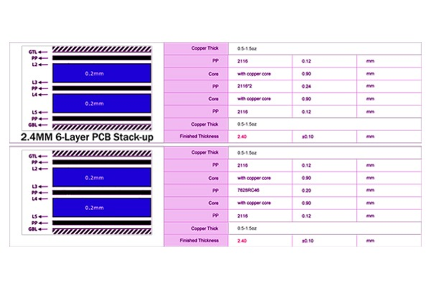
TUOGEE’s 6-layer PCBs feature optimized stack-up designs to further reduce transmission loss, meeting stringent requirements for 5G and AI applications.
Common Materials & Properties
FR-4 Epoxy: Cost-effective, suitable for most consumer electronics, withstanding 130-140°C.
High-Frequency Materials (e.g., Rogers RO4350B): Low dielectric loss, ideal for 5G base stations and radar systems.
High-TG Materials (TG170+): Heat-resistant, perfect for automotive and industrial control systems.
Metal-Core (Aluminum): Excellent thermal conductivity, used in LED lighting and power modules.
TUOGEE offers full material customization to precisely match your performance requirements.
Core Manufacturing Processes
TUOGEE operates Class 10000 cleanrooms with fully automated production lines, achieving >99.2% yield rates.
Key Application Areas
TUOGEE has delivered 6-layer PCB solutions to 500+ global clients with an annual capacity exceeding 500,000㎡.
Common Issues & Solutions
Issue 1: Layer Misalignment
▶ Solution: X-ray drilling positioning system achieves ±25μm registration accuracy
Issue 2: High-Frequency Signal Loss
▶ Solution: Ultra-low profile copper (RTF/VLP) with hybrid stack-up designs
Issue 3: Post-Solder Delamination
▶ Solution: Pre-baking + high-TG materials improve thermal cycling resistance 3x
Issue 4: Impedance Mismatch
▶ Solution: Real-time dielectric monitoring + adaptive compensation algorithms
TUOGEE provides end-to-end technical support from design to mass production.
About TUOGEE
As a premium PCB manufacturer, TUOGEE specializes in 6+ layer boards expertise, featuring:
Contact our engineers today for customized 6-layer PCB solutions!